Search
Close this search box.

Atomic Edge Passivation Deposition Complete Solution

Atomic Edge Passivation Deposition Complete Solution

Atomic Edge Passivation Deposition Complete Solution

Description (Laser Dicing)

Non-destructive laser dicing adapts concept of precise controlled heating in pair with localised cooling technique to create a temperature gradient, which will create thermal stress in the substrate, and the substrate will break once it reaches its fracture threshold. The crack propagates along the thermal gradient induced by the laser beam path, leading to complete clean separation of the substrate.

Description (EPD)

To deposit an AlOx passivation layer on the edges of the laser cut edges via ALD process, suitable for TOPCon cell applications.
Parameter
  • FunctionLaser dicing
  • Wafer size compatibleLength 182-230mm; Thickness 110-230um
  • Throughput≥12000pcs/h
  • Breakage≤0.02%@182;≤0.03%@210
  • Uptime≥98.5%
  • Laser PowerContact Opening ≥50W,Dicing ≥300W
  • Laser performancePower stability ≤2%RMS,annual degradation <3%
  • Dicing precision±0.1mm
  • Defect inspection≥0.5mm*0.5mm
  • Water consumption<1L / every 10,000 wafers
EPD film deposition distribution at various position

Atomic Edge Passivation Deposition Complete Solution

EPD Parameter
  • Uptime99%
  • Loading21600 half-cut
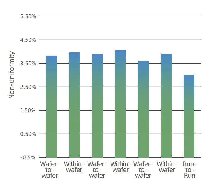
  • Non-uniformitywithin-wafer & wafer-to-wafer ≤4%,run-to-run≤3%
  • Temperature control4-segment heater:12 zones independant temperature control,compatbile for 400℃ annealing process
  • ProcessTube-type ALD,TMA+water
  • ConfigurationVarious online/offline solutions depending on the needs of customer
Module Power Gain
  • Power Gain+5.2W
  • Voc Gain+0.088V
  • Isc Gain+0.008A
  • FF Gain+0.41%
Description (Test & Sort)

Atomic Edge Passivation Deposition Complete Solution

Parameter
  • Throughput≥7200 pcs/h(half-cut)
  • Uptime≥98.5%(100%-machine failure)
  • Breakage100um-145um ≤ 0.1% (Broken pieces/input wafers)
  • AOI ResolutionEdge chipping: 120um x120um Stain, foreign objects :200umx200um
  • Voltage Test Resolution0.0001V
  • Current Test Resolution0.0001A
  • IV variation (Sweep Mode)Sweep-mode variation <0.05%,steady-state variation <0.02%,Each sweep EFF max range ≤0.05%
  • Min. EL detectable size0.5mm*0.5mm
  • Class Binning≥120 bins (single side)